K & S Dicing Saw

June 2nd, 2011


K & S 7100 dicing saw

Brief history

The K & S company was founded by Fred Kulicke and Albert Soffa in the 1950s as a custom engineering business.  Working in the beginning by designing automated solutions to different demands from all aspects of industry including stuffing sausages and cleaning beer cases.  This company rapidly developed an excellent reputation for being innovative and reliable.  Once the first semiconductor chip was developed they saw and took advantage of the opportunity to offer solutions to manufacture these chips.  Their major role was initially in the wire bonding aspect; developing excellent solutions in this area.  Later they expanded their contribution by making semi automated equipment for wafer fabrication and preparation as well as wafer dicing machines and tools.  In this area is where the company developed to be great and where they offered their most important contributions.

Contributions to the industry

Aside from the machines and dicing blades they have also contributed tremendously in techniques and theory.  As a machine operator, writings such as “Principles of Dicing” and “Dicing through hard and brittle materials in the micro electronic industry” by Gideon Levinson have at the very least influenced me personally.  Undeniably, their major contribution to dicing in particular, has been their equipment.  Being one of the first companies to offer the right equipment and tools to do the job and improving tremendously as time passed.

The K & S dicing saw

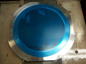
In the image at the top of this post you can see the K & S 7100 dicing saw which we have in our facility and use regularly.  This machine is capable of processing up to 6″ wafers.  It utilizes 2″ blades and can spin them at up to 60K RPM.  This machine is in our production floor cutting all types of materials from silicon to quartz.  It is versatile and it is equipped to do contact and/or optical height sensing.  It has pattern recognition and can be programmed to cut all types of dicing schemes.  This machine and others of its caliber are the legacy that this company has left for this industry and in particular for our dicing needs.

Source for k&S history from:   http://www.fundinguniverse.com/company-histories/Kulicke-and-Soffa-Industries-Inc-Company-History.html


How to mount a wafer on dicing tape

May 4th, 2011

The picture is now getting clearer and the puzzle is beginning to take shape.  Many aspects of the dicing process are in light but there is still a lot to cover.  On this particular post, I would like to talk about how to mount a wafer or substrate on to tape in order to get it ready for dicing.  I have written about what tapes are available and what are the parameters that determine the thickness, tackiness, and type of tape to use.  Once it has been decided on the ideal tape the next step is to actually mount the wafer.

The ring

There are two main mediums which are widely used to hold the tape and hence the wafer in place.  One of them is a ring.  This is a plastic hoop composed of two parts.  This ring is much like an embroidery ring made of plastic and it holds the tape in the same way the embroidery ring holds the cloth or fabric that is going to be worked on.  Basically it utilizes a small and large diameter ring that assemble together holding the tape in between while slightly stretching it once its in place.  This is the ring that you see on the video above.  There are a variety of ring sizes in order to accommodate the different sizes of wafers.  The one in the video is an 8″ diameter ring that is used for 6″ and smaller wafers.

The film frame

Film frame on a machine work table

Film frame on a machine work table

The second medium that is used to hold the tape is whats called a film frame.  This is a metal frame that is widely used in some applications.  Mainly to accommodate some machines and systems that only accept this type of medium to hold the wafer on the table or work area.  It is basically a round metal frame that is roughly .050″ thick with notches at the bottom that assemble in the work area of the machine like I illustrate in the pictures above.  As opposed to the ring, the film frame is only composed of one piece of metal and the tape just adheres to the inferior side of the frame.

Mounting

Whether it is a ring or a film frame that is used to process a wafer, the mounting is absolutely crucial.  In the video I show the technique used to do this manually.  It is paramount that there are no air bubbles in between the tape and the wafer because this will cause many problems during the dicing.  These problems could amount to blade or material breakage and/or pieces of the material falling off the tape.  Since a vacuum is used during dicing one can see how the material can break once it is activated if there is a lump between the tape and the wafer.  If the blade passes through the part with the air bubble and the piece comes off, it could break the blade or it could scratch the rest of the wafer.  In order to avoid air bubbles and to ensure a proper mounting, the technique requires that the tape is placed close to the wafer without being in contact with it at first.  Using the digital pulp of the finger the tape is then carefully pressed onto the wafer making contact and adhering to it.  Starting at one extreme of the wafer and slowly working across it until the mounting is complete.

Now that the wafer is mounted, be it on a ring or a film frame while using the right tape, it is ready to be diced.  This is where the parameters and the machine come into play.  There are many types of processes that can be used such as scribing, notching, and dicing all the way through the material.  I will discuss this further in a later entry.  Thank you for your time.

Techniques on how to dice extra thick materials

January 27th, 2011

As you may have read on this publication or perhaps noticed in the current trend in our technology, everything is becoming smaller.  There are however certain applications that require the dicing of extraordinarily thick materials.  This is the case of such materials as glass, quarts, ceramics, and some silicon.  These applications range from making imprint masks, to making heat shields, and substrates that require an unusual or uncommon thickness.  To put this in perspective the current standard thickness for any given material in the industry is about .021 – .029″.  We are in this article talking in specific of thicknesses of .100 – .250″.  When encountered by these types of thicknesses one faces a new set of challenges.

The first challenge, from the dicing point of view, is the blade thickness and exposure.  It is likely that when dicing something that is 1/4 of an inch in thickness, a 3 or 4″ diameter blade is needed.  Also the thickness of the blade needs to be relative to the thickness of the material.  The blade needs to be fairly thick in order to accommodate the spindle load that will be generated.  A thickness of .020 – .030″ is recommended for the blade.  Now there are a couple of different techniques that one might use to accomplish this task and they will require different procedures  as well as yield different results.

Multiple passes

In fact, it is recommended that when dealing with thicknesses of .060″ and over, the dicing be done in multiple passes.  This technique requires the blade to make several passes while gradually cutting the whole of the material.  In other words the blade makes the first pass at say .015″ into the material; on the second pass it knocks out another .015″ and so on until the blade reaches beyond the tape and the cut is completed.  This is very time consuming since for every cut that needs to be made, it has to be multiplied by the number of passes.  Thats the obvious problem but another is that, when dealing with extraordinarily thick materials, the blade tends to deviate during the first passes because of lack of support.  Along with the spindle load created while trying to cut through this material and the amount of exposure that is not being used, it is the perfect recipe for wavy cuts.

This can be remedied by using a different scribe blade.  Instead of using a blades that gives you the entire exposure needed, we recommend using one that has only about .050″ of exposure.  Scribe .040″ into the material and make the trenches for all the cuts that need to be made.  Once this process is done, switch to the blade that has the entire exposure and dice in multiple passes over the trenches that were created earlier.  The second blade will tend to follow the scribe cut alleviating any waviness.

Another issue is the bottom of the cut or the back side chipping as we call it.  It tends to be augmented when dicing thick materials.  Some of the causes are, improper cut depth,  improper RPM or feed rate, and vibrations that occur while the last chunk of material is being knocked off on the last pass.  There are no real cures for this, backside chipping is an immortal archenemy of dicing.  To improve these unwanted happenings the right thickness of tape is required in order to acheive proper cut depth.  Preferably a tape that is sturdy and does not allow for much vibration.  We recommend using a RPM of 15K for 3 and 4″ diameter blades.  20K for 2″ blades and a feed rate of about .02″ per second depending on the specs and material.  For glass and quarts we recommend using 325 grit size, for ceramic 270;  and for silicon 3000 or larger.

Cutting from both sides

This second technique is our finest weapon for fighting backside chipping, but in turn it requires extreme precision and it often produces results that might or might not be an issue to the final product.  This process essentially requires that the material be scribed from both sides.  This, as I said, is very efficient at reducing or in some cases eliminating back side chipping simply because the blade never dices through the entire thickness at once.  In this process there is only need for enough exposure to dice say 2/3 of the way through the material.  The wafer is mounted normally at first, aligned and scribed past the half way point of the wafer thickness, making all the cuts necessary.  After that part of the process has been done for the whole wafer, it needs to be unmounted, flipped, then mounted with the scribe cuts facing the tape.

Here comes the tricky part!  Then the cuts need to be finalized from the other side of the wafer.  Once the wafer is at this stage the blade can easily knock off the rest of the material without having to go all the way through the entire thickness, hence eliminating the horrid back side chipping.  There are several ways this can be done accurately.  The easiest way is if the material is glass.  In this case it is not difficult to focus on the bottom of the cut with the optics so that proper alignment is achieved.  In case of non see through materials there are 2 steps that can be taken.  1) While the wafer is still on phase 1 of this process, precise measurements need to be taken from the edge of the wafer to the center of the first cuts both on the X and Y directions.  When the wafer is flipped these measurements can be used to blindly find the center of the first cut and from there the rest of them.  This poses two problems, first, that the measurements need to be very accurate and second, that the machine has to be very accurate as well.  This ensures that perfect alignment is made with the initial trenches which are invisible because they are now on the back side of the wafer.  2)As an alternative, when the wafer is on phase one, the first cut of both the X and Y directions are completely made while the rest of the cuts can be made as previously expained.  The edge of these first cuts can be used as reference points when the wafer is upside down.

Dicing this way I have to admit, and worn, is not always advantageous or simple to do.  However there are many applications that could benefit from this technique, especially because if it is done correctly it is a sure way of getting only front side chipping both in front and back of the material which is always significantly less than the back side chipping.  A major issue with this process is that if improper alignment is done the cut profile will not be adequate, now in some applications this is a don’t care and getting the backside chipping diminished is more important.  Also this technique will definitely not work for any wafers that cannot be touched on the front side for it requires the wafer to be mounted top side down on the tape.

Having used both these techniques on many projects for many of our customers, whom will not be named, we have confirmed that they are sound techniques.  However it cannot be stressed enough that at least the second one is not for everyone and encourage the reader to look closely at their requirements to see if these procedures are for them.  A lot of dicing houses will not even consider dicing this way due to the amount of time and personal attention that these type of jobs require.  It is likely that a house that is focused on mostly production runs will not take their time to process a small lot of wafer this way.  If the reader has a question whether these processes will work for their application I would be happy to help asses this issue and can be contacted through my email.

I would also like to thank the readers once again for their time and feed back.  It is true that words are meaningless unless they are thought to have meaning and relevance by the reader.  Fortunately there are enormous amounts of people who are curious as to how their favorite devices come to be and the processes that make them possible, even if they are hidden.  Thank you.

The integrated circuit and the dicing process

November 13th, 2010

The making of the integrated circuit is a long and arduous process that involves various steps and procedures.  In most cases the wafer, as its called, travels to different locations before it is completed and turned into the final product.  This 6, 8, or 12″ diameter wafer houses maybe thousands of tiny instruments.  Devices that have been created as part of a bigger creation or as key components to perhaps the next scientific breakthrough.  The wafer designs vary in complexity but can be as complex as utilizing various types of materials; from gold to copper, germanium to gallium arsenide.  Wafers with soldier bumps or perhaps an intricate run way of channels and cavities.  Wafers that are made up of waveguides or actual moving parts such as MEMS and much more.  I will dare to say that the possibilities are inexhaustible.  The microchip is truly an attribute to human kind and our hunger to better ourselves in this new technological era.  With the following words I would like to offer a simplistic overview of the process while focusing on how dicing comes to play and why it is so important.

Making the silicon ingot

This process is done in a crystal pulling furnace where high purity silicon is melted in a controlled environment.  Then a single crystal silicon seed is introduced, rotated and slowly pulled allowing the atoms of the pure silicon to attach to the crystal seed forming a single crystal ingot.  This is a slow process with many different components such as precise temperature control as well as different kinds of dopants and  pure gases to achieve the desired specifications.  Needless to say, the furnace is a complex piece of machinery composed of many elements that ensure precision.   This ambient is the birth place the silicon wafer!  The fundamental base for most integrated circuits.  Once the ingot is produced, it is polished and the crystal orientation marked by making a notch or cutting a flat on it.

Slicing and polishing

The ingot is them sliced using a wire saw or an inside diameter saw to create a wafer that is uniform in thickness.  The lapping and polishing processes are done to achieve the right thickness and to eliminate any imperfections that may be present in the rough wafer.  The wafers can be single side or double side polished.   The polished side of the wafer is the side that will be used to make the circuitry required for any specific device.  The edge of the wafer is also polished and rounded off to prevent breakage.  After this the wafers are rigorously cleaned using a variety of solvents and deionized water, then dried.

Oxidation

This step is extremely important in the manufacturing of the integrated circuit.  Coincidently it is a natural occurrence in silicon over time, but this process is accelerated using either oxygen or water combined with very high temperatures.  This is done in an oxidation or diffusion furnace where the silicon is exposed to one of the two elements depending on what type of oxidation you want to achieve.  The elements react with the wafer forming a thin layer of silicon dioxide.

Photo-lithography and the etching process

Now its time to make the circuitry in most cases composed of transistors, capacitors, resistors, and connectors.  Keep in mind that these are made in minuscule scale for the trend has been for smaller and smaller devices over the years.  How is this done?  Well as the name of the process suggests, this is done by borrowing techniques from photography and lithography.  First the wafer is coated with photo resist which is a light sensitive liquid material that is applied while the wafer is spinning to ensure an even coat.  The wafer then goes through a soft bake in order for the resist to cure.  A mask is made from soda lime or fused silica.  This mask contains a large scale outline of the circuitry or pattern that is intended for the wafer.  The coated wafer will act as the photographic paper and the mask will act as the negative.  Ultra violet light passes through the transparent areas of the mask onto the wafer and the resist will react to this light.  After this the wafer is developed using chemicals that will remove the exposed photo resist.  The wafer then goes through an etching process where the oxidation layer that is not protected by the resist will be taken off.  Finally, once the resist is no longer needed, it is removed using more chemicals.  This process is repeated as necessary to achieve the wanted results.  Once the wafer has been completed it generally goes through some tests to identify the working and nonworking devices.  A map or a drawing of the wafer is made identifying these and sometimes the bad devices are marked on the wafer.

The dicing process

Now you have hundreds or thousands of microchips in one wafer and the only thing that stands between that wafer and the final product is a few more steps.  The first thing to do now is to separate the devices from each other and this is done in the dicing process.  The dicing process is a violent and dirty process by which a blade made out of diamonds bonded together by nickel, resin, or metal spin at very rapid RPM, while the wafer is driven into it at a predetermine feed rate.  Dicing is a lot like cutting tile but at a smaller scale and with much more precision.  In most cases a small space called a ‘street’ is accounted for in the design so that a fine blade could cut through without touching or harming the actual device.  Normally the street is about 80 microns in width but this may vary and the trend is for smaller and smaller streets .  In actuality with nickel bonded blades, which are the standard for dicing silicon, we can get a minimum thickness of 15 microns or .0006″.  The three most important elements in dicing are: the blade, the machine, and parameters.

The dicing blade

Choosing the right blade for any particular application is crucial.  These essential precision tools come in a variety of sizes, types, as well as in different abrasive or grit sizes.  They also come in hubbed and hubless forms.  The different types of blades are: resin bond for dicing glass, quartz, sapphire and such materials.  Nickel bond for dicing silicon, gallium arsenide, germanium and indium phosphate.  Metal sintered blades are good for dicing plastics, QFN packages, PCB and FR4 type materials.  They all utilize diamond as an abrasive and the diamond (in most cases synthetic diamond) is what does the actual cutting.  The key is in choosing the right size diamonds for the particular application at hand.  When dealing with hubbed blades the exposure is to be considered to ensure that there is enough blade to cover the material and sufficient room for wear.  When dealing with hubless blades the flange needs to be taken into account.  The flange is a metal hub that holds the blade in place and sets it in the spindle.  In choosing the right hubless blade one needs to keep in mind the ID and OD of the flange to determine the right size blade that is needed.  The exposure of a hubless blade is determined by subtracting the OD of the blade from the OD of the flange and dividing that number by 2.  The essential specifications for a blade are size (ID, OD),type(nickel, resin, sintered, hubbed or hubless), thickness, grit size, and exposure.   Some manufacturers use different diamond concentrations and that is to be acknowledged as well.

The dicing machine

The dicing machine has evolved over the years to be very complex and accurate; in most cases with tolerances of 2 – 5 microns.  It is composed among many other things of a spindle, which can come in 2, 3, or 4″ sizes; the 2″ is the most common.  The spindle is attached to a ‘lead screw’ which allows it to move in the Y direction.  It also moves up and down in the Z direction.  The chuck, which also utilizes a vacuum, is a metal or ceramic table that moves in the X direction and it determines the feed rate.  In other words the table is what drives the wafer into the blade while it spins and does the cutting.  The chuck also rotates which is essential for alignment.  In order for the wafer to be diced, it needs to be mounted using a ring or film frame and dicing tape.  Then the wafer can go on the chuck and the vacuum is activated to prevent it from moving during the violent process.  The blade is set to cut just slightly into the tape without going all the way through.  This is done so that the wafer is diced completely while the tape remains intact.  Among other hardware, the dicing machine is composed of optics that let you see the pattern on the wafer, as well as software that allows for programing according to the specific dicing need.  The newer models come with such technological marvels as pattern recognition and automated wafer loading and unloading.  As well as sensors that will perform automatic blade hight adjustments and compensate for wear.

The parameters

In dicing, parameters are paramount.  The important parameters are as follows: RPM, feed rate, blade type and grit size, cooling water, and number of passes.  These are determined by, material type, material thickness, street width, as well as chipping tolerances and die size.  It is also very important to choose the right tape as explained in a prior post.  The right combination of these parameters will ensure that the final product is a success.  As time progresses the streets get smaller, specs get tighter and the over all demand for a more accurate dicing has increased.  If any of these parameters is off or not adequate there will be mortal consequences for the device, such as unacceptable front side and back side chipping, improper cut profile or cut depth, cracks, dirtiness, or mis-cuts.

Cleanliness

I mentioned this process to be a dirty one because during the dicing, the silicon wafer exudes great amounts of saw residue which gets all over the place.  In order to keep the devices clean one of two steps are taken.  1)The wafer is coated with photo resist prior to dicing, which is applied to the wafer like I have explained earlier, then it is baked at 100 degree Celsius for 30 minutes.  Any residue that attaches to the surface of the wafer is taken off when the photo resist is removed.  2)The wafer goes through a cleaning procedure in a specialized pressure washer after dicing.  This is a high power pressure washer that basically shoots deionized water at the diced wafer while it is spinning, eliminating any saw residue that might be present in the crevices of the wafer.  This process is usually the last after the dicing is done and the wafer is ready for the next phase.  If the photo resist option was applied, then the final step would be to clean the photo resist off the parts with a process that I will discuss at a later entry.

Pick and place; final packaging

Finally after this long enterprise and having sent the wafer through all these different procedures, the microchips are made and diced.  However they are attached to dicing tape on a ring or film frame and there is still one final step.  That is to remove all these individual instruments off the tape and package them for sale or assembly.  This is done by the pick and place process.  There are two main ways of doing this; manually or in a fully automated process.  To do it manually a vacuum wand is used which is basically a pen like instrument that utilizes a vacuum to suck the die pieces off the tape.  The wand has a release mechanism that lets you place the die pieces where necessary.  Each individual die is picked and placed in a gel pack or waffle pack.  The gel pack is a container which has a sticky membrane at its base and they come in various tackiness levels that essentially hold the device in place for transportation.   The waffle pack is different in that it only has the cavities large enough to fit the individual die with no adhesive what so ever.  The automated option is with a machine that can be programmed to pick any given array of die off the tape.  In order to pick the right die, whether it is done manually or automatically, the drawing or map of the wafer is used as a reference to locate the working die.  Then the microchips are off for final packaging or assembly.

My hope is that after reading this, the reader obtains a better understanding of this complicated process and in doing so he or she can see what goes into making the devices that make our lives so great.  The integrated circuit has become a part of our daily lives and it is present in things such as our phones, computers, our cars and more.  It is an essential component in our defense, our communications, and our entertainment.  It is a key that has opened innumerable doors for humanity in the medical, technological, and scientific fields.  It is the technological impulse that has catapulted us from a primitive past and into a great and intriguing future.  Moreover the integrated circuit continues to evolve and become more efficient, making the present and future an exciting thing to think about.  The thoughts of where we have come from in 50 years and where we will be at 100 years from now, thanks to this minuscule apparatus, makes us quiver with fascination, nostalgia, and wonder all at the same time.  Thank you for reading.


Dicing Tapes

September 11th, 2010

Selecting the right dicing tape is crucial for the dicing process.  The right or wrong decision can make or brake  a project.  As you may be aware there are so many different choices, there is bound to be a tape for almost every application.  The important thing is to know the different characteristics of a particular tape and how it can be beneficial or counter effective for what you are doing.  There are two main categories when it comes to dicing tapes: Standard or UV release.  Most tapes are PVC based films and the adhesives that they utilize are acrylic.

Standard tapes: These tapes are usually blue in color and they do not have a backing film.  Which means that as you peel the tape the adhesive is exposed.  These tapes come in different thicknesses, from 80 microns to 130 microns, as well as different tackiness levels.  The adhesion level is measured in g/mm; the larger the number of grams, the tackier the tape is.  Mainly the difference between these tapes and the UV release tapes is that standard tapes do not need to be exposed to UV light in order to release the part.  This can be beneficial and not, depending on the application.  For example if you have a silicon wafer which is very thick and it is diced into very small pieces on standard tape there is a high probability of the pieces coming off the tape during the dicing process (disaster).  On the other hand if you have a wafer which is standard thickness and it is to be diced into relatively large pieces, it can be easily diced on blue tape and the pieces can be taken off the tape without a problem  and without UV exposure.  The type of material also needs to be taken in consideration since some materials are not so easy to adhere to.

UV release tapes: These tapes are usually clear in color and they come in many different thicknesses as well.  UV release tapes have a backing film which needs to be peeled off the tape before applying it to the material.  They also vary in tackiness before and after exposure to UV light.  This is important because in the event that you have a very thin wafer which needs to be diced into relatively small pieces, but the g/mm is high even after the exposure, you will still have problems picking those fragile pieces off .  Generally the UV release tapes are good when you want a strong adhesion during dicing but an easy release once exposed.

The thickness of the tape you choose  is very important because you want to make sure the appropriate cut depth can be achieved.  Making sure of this will alleviate all sort of problems in the final product.  How can you determine the right tape for you ?  The guidelines are: material, material thickness, desired cut depth, blade thickness, and final die size.  When you take in consideration these aspects it will help you to determine the right tape for your specific application.

An important thing to remember is that most of the tapes, whether they are standard or UV release tapes, need a curing time.  This means that they need to sit for some time ( at least 4 hrs ) before dicing.  This allows the adhesive to fully grasp, if you will, the material that needs dicing.  In countless occasions I have heard people complain that their parts are coming off the tape when they mount the wafer and start dicing right away.  Another thing that causes this is air bubbles that remain in between the part and the tape.

This subject is very difficult to cover and it definitely requires some homework from the user point of view.  I recommend talking to your provider of dicing tapes so that you may discuss the different options available to you and from there decide on the best one.

On another entry I will discuss another popular mounting technique which is the use of thermal bonding agents other wise known as crystal bond.

Synova micro jet laser

September 10th, 2010

This is a Synova Micro jet laser system cutting some resin bond material.  It is a 1064 nanometer wavelength laser and it can be programed using CAD/CAM to cut any pattern.  This is what we use to cut our custom blades whether they are resin or metal.  This laser has its set backs, such as not being able to cut through some materials due to its frequency and that the minimum kerf available is 80 microns.  How ever it can cut through materials like stainless steel, SiC, Si, as well as soft material like graphite.  So the application is completely dependent on the wavelength and the material’s willingness to absorb this particular frequency.  It has been very useful in making special blades, for example blades with a specific number or  a particular shape of slots.  We’ve actually had a customer in the past commission a blade with a very unique set of slots, almost like a serrated resin bond diamond blade.  This laser’s main application as of now is the downsizing of wafers and wafer dicing, but its advantages far outweigh its limitations for sure and its total uses and applications in my opinion are underestimated and unexplored.

Grand Opening of our online store

July 29th, 2010

We are proud to announce that our on line store Blades Overnight is now open to the whole of the United States and Canada.

In our store you will find a wide selection of dicing blades both resin and nickel bonded.  With an assortment of different mesh sizes and thicknesses.

The link is:www.bladesovernight.com, so be sure to check it out!  I am sure you will find what you need for your next dicing necessity.  We offer a large selection of blades for most all applications.

The best part is that the blades shown on our site are from our in house stock, so we are able to ship same day if the order is placed before 12 noon standard pacific time.  Please check it out and let me know of any feed back you may have.

On a different but related matter, I want to thank all the people who have read my posts and commented.  Your comments are greatly appreciated.  After a short leave of absence I will continue to post on dicing related topics.  Thank you for reading and I look forward to the next one.

CBN versus Diamond pictures

May 20th, 2010

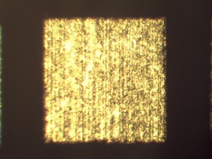
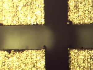
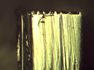
top view of Kovar diced with diamondtop view of kovar diced with diamond bladeside view of Kovar diced with diamondtop view of Kovar diced with CBNtop view of Kovar diced with CBN bladeside view of Kovar diced with CBN

CBN versus Diamond

May 20th, 2010

What is CBN and how does it compare to diamond as an abrasive?

This is an interesting question in the sense that you cannot reach a concrete answer.  In other words you cannot say that one is better than the other.

How ever we have done some experiments that show that CBN outperforms diamond in certain applications.

Cubic Boron Nitride is a synthetic abrasive that is not soluble in alloys like nickel and iron.  It can withstand higher temperatures than diamond although it is not as hard.  Since diamond is soluble in ferrous alloys CBN is great at something diamond is not.

For the experiment we have used Kovar material which is a nickel-cobalt ferrous alloy.

When diced with diamond the burrs on this material are enormous and the cuts look very ugly.

The CBN blade seems to dice through this material with much more ease.  The cuts look much better  and the burr diminished significantly.  We measured an average of 21 micron burr with CBN compared to 150 micron with diamond.

The pictures taken with our high power microscope illustrate this perfectly.

In conclusion CBN might not be better than diamond at everything but it is certainly much more effective with ferrous alloys.  CBN has the same success for these type of materials than diamond has for materials like glass, quartz, sapphire, and ceramics.

Further test will follow to determine the best CBN grit size for materials like Copper, Nickel, Titanium, Silver, and Aluminium.

Slotted Blades

May 3rd, 2010

Here is a picture of one of our slotted resin blades.  The slots can be added to any of our hub less blades and they have proven to significantly reduce smearing of malleable materials such as gold and silver.  It also has better cooling characteristics because the cooling water is able to get into the slots making it run cooler over all.  The slots can be added to our sintered blades as well, improving their already goon performance on materials like FR4 and plastics.